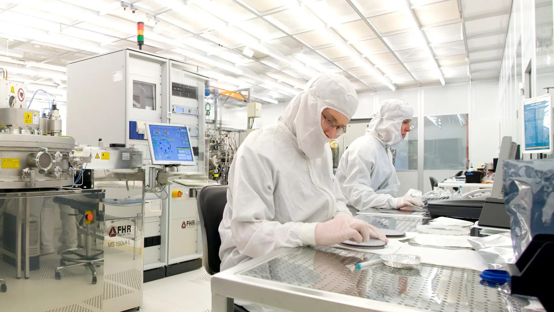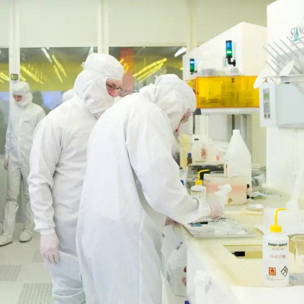
The laboratory is an open user facility for external as well as internal academic and industrial interests. The Nanofabrication Laboratory offers a broad platform of process tools for the development and testing of new ideas in micro and nanotechnology.
Two strategic focus areas in the cleanroom are within quantum devices and microwave/photonic devices. Both rely on our strength and strong heritage within nanoscale lithography.
The Microwave and Photonics Processing Line encompasses a complete set of process tools from material growth to packaging where either access is limited to microwave or photonic devices or where only approved processes can be run. The Line supports complex fabrication of high-quality III-V components with fairly large number of mask layers, such as transistors, varactors and lasers.
In a similar way the Quantum Device Line supports fabrication of state-of-the-art quantum devices such as single electron transistors and qubits.
The nanofabrication laboratory has 193 process tools available for fabrication and characterization at the micro/nano-scale.
Head of laboratory and staff
Publications in Chalmers Research
We continually document our research in various types of publications, which are registered in Chalmers Research. Follow this link to see recent publication lists

Myfab Chalmers
The Nanofabrication Laboratory is a clean room facility for research and development in micro and nanotechnology. You will find a wide range of equipment for developing and testing new ideas on a micro and nano scale here. The laboratory is part of the national research infrastructure Myfab, which is coordinated by Chalmers.
Head of laboratory
- Head of Division, Nanofabrication, Microtechnology and Nanoscience
